PCB assembly is a procedure of mounting different components on the Printed Circuit board surface such as connectors are linked electrically or through copper wires called traces. JLCPCB has launched a free PCB assembly service to facilitate customers. Special offer of 0$ for multilayer (1-4 layered) PCB assembly.
Place your order for free PCB assembly:
- Save Gerber file:
Make up your schematic diagram of your desired PCB and save it as a Gerber file. Sign in to JLCPCB and upload the Gerber file by clicking order now or Quote now options.
- Add Geber file:
Select ‘order now’ and click on ‘Add your Gerber file’ you can upload your Gerber file of PCB in JLCPCB.
- Enter details:
Select your favorite PCB manufacturing details like size, quantity, layout, layers, and thickness, etc.
- Generate and upload BOM file:
BOM file will tell the manufacturers about the values of the components like capacitors and resistors for PCB. BOM files contain respective properties of PCB components in CSV format of simple text file, but MS excel or Google docs can be used to generate BOM files.
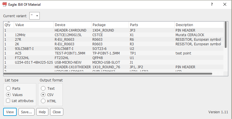
- How to generate a BOM file from Eagle?
To generate a BOM file from Eagle you will have to make sure that you are using and in the “Schematic Editor” and go to File > Export > BOM. It will open up a window where you can set the interface of the BOM file as to how the BOM file will look like, then check the “Values” option and uncheck the “List attributes” option, next to it you can save bom.csv to the desired location you selected by clicking “Save” button.
Now columns can be added in the file for the JLCPCB system to accurately identify it.
- How to use Google Docs?
Start by creating a new spreadsheet and then go to File > Import, then select upload and select the created bom.csv file. Here you can select either to replace the existing sheet or to create a new one. The correct separator should be selected, and click on import data.
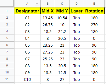
- Generating CPL/pick and place file:
For generating this file ensure that you are in the board editor the click on File >Export > Mount SMD, this will open the browsing option and will prompt twice as to where to save this file, first for top assembly, save it as a top.csv file and second prompt for the bottom assembly file, save it as bot.csv.
As being generated by Eagle CAD so the file is not in expected format by JLCPCB so changes must be made, Create a new spreadsheet and go to File>Import, select upload, and select previously created CSV file.
- How to edit Data?
If individual columns are not identified correctly then select the Data>Trim Whitespaces, nest goes to Data>Split text to columns and select the appropriate separator. Excess columns can be deleted and required columns can be inserted where needed. You can name their Header as the first header would be designator, second would be X position and Y position, third would be layer column as to top or bottom layer and next would be orientation column as needed by JLCPCB.
- How to export it from Google Docs?
Click on File>Download>Comma-separated values. Name this file as assembly.csv and then upload it when you are ordering the SMT assembly service along with the BOM file.
- Check free PCB assembly /SMT assembly
Check ‘free PCB assembly for your PCB order’ and select a few desired options after reading the instructions carefully. You can choose PCB parts from the JLCPCB parts library.
There you can select a different option for your PCB SMT assemblies such as layers, thickness, color, surface finish, and quantity.
- Stenciling
Pick out stenciling properties for your PCB. You can select framework, dimensions, size customization, and stencil side as you want.
- Finalize order:
After selecting and checking all your needed properties for your PCB you can finalize the order by saving it to the cart. JLCPCB ships PCB all-around the world by choosing the options available for shipping service.
- Checkout:
After clicking save to cart, you can place your order for shipping at your doorstep. Click on ‘checkout security’ add your address and continue selecting the shipping method. By clicking ‘submit order’ you can enter your payment method. You can add a coupon or promotional code here and apply for more special discount offers.
- Good to go:
Select and confirm the payment method and you will get a conformational email shortly containing all your information regarding the respective order.
In case of any problem, you might get another email referring to the problem JLCPCB faces while manufacturing your PCB. To resolve the respective issue this method is very feasible so that the company can proceed with making and shipping your desired PCB.
Get free assembly for your PCB:
JLCPCB provides a $24 coupon to every customer for SMT assembly on monthly basis. Three coupons as $9 + $9 +$6 will be available for customers after placing an order. You can check SMT coupons from your JLCPCB account in the ‘Coupon’ section.
When you checkout, select a $9 SMT coupon, and the discount will be automatically applied during checkout. Which can cover the $7 setup fee, $1.5 stencil fee, and the SMT assembly starts at $0.
JLCPCB assembly capabilities:
- Types of assembly:
- SMT (surface mount technology):
SMT refers to mounting or placing PCB components directly on the board. SMT processing allows faster, efficient, affordable, smaller, and lighter PCB to fit in most electronic devices. SMT is also called planar mounting. Components used for direct mounting are called SMDs (surface mount packages/devices).
SMT PCB by JLCPCB
JLCPCB uses modern and efficient machinery to carry on the process, such as a pick and place machine used to place and mount the components accurately at their position.
- THT (through-hole technology):
In this method, Different components are mounted on the Printed circuit board through holes drilling and fixed with lead. Various soldering processes are used to fix the lead components on the board like iron soldering, hand soldering, or wave soldering.
Two main types of components are used in through-hole mounting called Axial and radial leads. Axial components are mounted on both marginal sides of the board whereas, the radial lead components are placed on one side of the PCB.
- Single-sided placement
Single-sided PCB is a basic model of PCB that has components or conductive copper fixed on one side of the board, and its conductive wiring is assembled on the other side. Many electronic products depend on single-sided PCB such as cameras, calculators, radios, printers, etc.
- Lead-free soldering:
JLCPCB proceed with lead-free soldering. In this kind of soldering method, different metals like tin, copper, indium, bismuth, and traces or some elements are used instead of lead. It demands a higher melting point (217o C) than simple lead soldering which causes quick oxidation of solder material. Lead-free soldering gives high fixation and joint strength and high resistance in PCB.
- HASL/HAL solder finishing:
Hot Air Soldering Leveling is used as a solder finishing process. PCB is dipped into molten solder material. In this way, all exposed copper surfaces are covered by solder completely. Excess of solder deposition can be removed by passing soldered PCB through hot-air knives. It is preferable for hand soldering. It leaves an uneven surface on PCB.
- ENGIN solder finish
ENGIN (Electro-less Nickel/Gold Immersion) is a lead-free surface finish that gives a smooth surface, brilliant soldering, and longer storage time. Better protection and to avoid oxidation electroless nickel and thin lining of gold immersion is used for PCB solder finishing.
Advantages of JLCPCB
- JLCPCB provides the facility of pre-ordering PCB parts through JLCPCB specialized warehouse. In-Stock extended parts have no minimum order limit but Non-stock extended parts require a pre-order with a minimum order quantity limit.
- PCB parts can be taken from the PLCSC warehouse where the Minimum quantity order limit is established and the price is estimated. Selected parts will be shipped to the JLCPCB warehouse, so the lead time will be longer than before.
- JLCPCB provides a secure checkout for its valued customers. You will fill up your details like your email address and contact details, these details can be changed whenever needed. Fill in your billing address and click “submit order”. As inventory changes vigorously, to make sure your order is shipped timely, customers should complete payment in one hour otherwise order will be canceled