Manufacturing
HDI PCBs or high density interconnect PCBs are special PCBs that have very compact and dense component placement and use either microvias, buried or blind vias. Such PCBs are one of the more complex PCBs to design and manufacture, further debugging problems in HDI circuit boards are notoriously difficult due to the compact and dense nature of the PCB. However, an overview of some common mistakes can ease the ordeal of debugging HDI boards. This article will give you a rough idea of why HDI is so mistake-prone, some common mistakes in HDI circuit boards and what can be done to avoid them.
Why are HDI PCBs More Prone to Mistakes?
HDI PCBs are quite sensitive designs that require advanced tools to design and manufacture, so much so that finding PCB manufacturers that support HDI manufacturing is also a task in itself. A few reasons HDI circuit boards are prone to design and manufacture mistakes are –
- Small Vias – The biggest reason HDI boards are difficult to manufacture is the size and types of vias that they usually use. Microvias, blind vias and buried vias require extreme caution and advanced techniques like laser drilling for manufacturing. Even a slight misalignment of any of these vias on any layer might cause an open or short circuit. Smaller vias by diameter tend to pose both electrical and physical problems if not designed properly.
- Difficult Inspection – They are required to go through a higher-resolution optical and X-ray inspection. Such inspections can catch very fine defects that may be considered “acceptable” for normal PCBs, but not for HDI circuit boards, thereby increasing the chance of an HDI board being called “defective”.
- Features and Footprints Used – They utilize fine-pitch components and techniques like via-in-pad. Such features increase the possibility of errors in assembly especially while soldering and desoldering components.
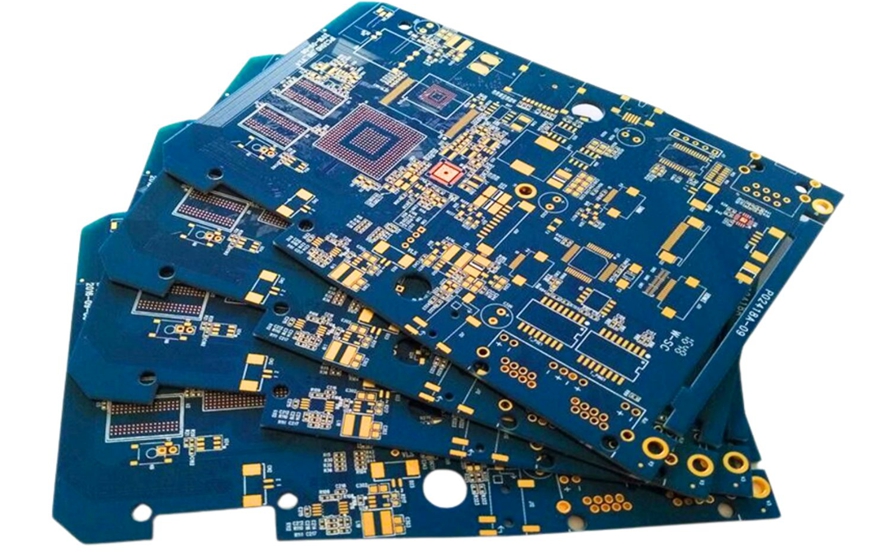
Some Common Mistakes in HDI PCBs
HDI PCB
HDI PCBs are prone to many problems and mistakes if not designed and manufactured properly. A few mistakes that may be committed in HDI circuit boards and how they can be avoided are –
- Improper Material Selection – Not all materials can support HDI designs, in-fact there are many expensive high-speed PCB materials that don’t support HDI. Some common PCB materials such as standard FR-4, standard polyimide like DuPont Kapton HN and a few PTFE-based laminates like Rogers RT/duroid 5880 do not support HDI features. HDI designs demand special materials that are compatible with HDI features and have tolerances and limits that have to be followed. Improper material selection can have severe repercussions like compromised physical and signal integrity, unreliable performance, etc.
To avoid such errors-- Read the material datasheet thoroughly and check for limitations and compatibility.
- Confirm compatibility of your requirements and material choice with your PCB manufacturer.
Improper Vias Design – Blind, Buried and Micro vias are required to maintain a certain diameter-to-depth ratio. These values are –
- Microvias – ≤ 1:1 and ideally close to 0.75:1.
- Blind and Buried vias – 0.8:1 to 1:1.
Not adhering to these ratios might lead to cracks and faults on PCBs and improper Via plating. Such errors can cause compromised physical and electrical reliability. Furthermore, too deep vias can reduce the efficiency and effectiveness of techniques like laser drilling.
To avoid such vias errors –
-
- Follow a very strict DRC check as such problems can easily be caught before fabrication with DRC checks before generating output files.
- Usually, the PCB manufacturer will warn you of such errors before the fabrication. As a precaution, confirming with your PCB manufacturer can give some assurance.
- Improper Thermal Management – They are quite dense and hence require thin vias and traces. In the case of power nets, they may not have sufficient width to support the required current, which may cause the traces to heat thereby affecting the performance of the components. The bigger problem, the PCB vendor will not be able to identify if the power net is sufficiently thick or wide and hence may not be able to warn about the same.
Such errors can be avoided by stringent DRC and running the designs through simulation software.
- Sequential Lamination Misalignment – Manufacturing of HDI circuit boards requires multiple lamination cycles. Any slight misalignment between the layers can be quite catastrophic due to the close placement of components and traces. It can cause open or short circuits causing a rework. However, such misalignment errors are quite rare and with modern fabrication tools such errors are quite rare and reputed manufacturers will usually detect the problem and rectify the error before delivering the PCB to the customer.
- Stackup Errors – Improper or incorrect layer stackup can result in many problems like increased crosstalk, and compromised impedance control overall contributing to poor signal integrity. Ideally, layer stackups are recommended to be symmetrical, which reduces the chance of errors and the chance of a phenomenon known as wrapping which is the bending or twisting of a PCB due to uneven thermal expansion, stress imbalance, or improper lamination. Stackup errors can also happen due to miscommunication or misunderstandings between the PCB manufacturer and the designer.
Different HDI PCB Stackup
To avoid stackup errors –
-
- Try to use conventional and common layer stackups that can be manufactured by most PCB vendors. (However, if you feel your design requires a special layer stack, go ahead with your layer stack since there are many PCB manufacturers that support custom layer stacks too)
- Ask the PCB vendor to confirm your layer stack and Gerber files before proceeding to fabrication. This step may increase your lead time but can drastically reduce the chance of stackup errors.
- Choosing PCB Manufacturer – There are plenty of manufacturers that claim that they can fabricate your specialised designs, however, many of them can be just middlemen who forward your fabrication files to another manufacturer which drastically increases the chance of errors and will most likely increase the lead time. Choosing the right PCB manufacturer like Viasion is quite an important part of the PLM of a PCB, especially complicated designs like HDI circuit boards. An experienced PCB manufacturer is most likely to maintain protocols and follow tough quality checks and can also help in choosing important aspects like layer stacks and materials that are equally crucial in HDI board designs.
Conclusion
HDI PCB requires scrupulous attention to manufacturing, design and even ordering the PCB. By following best practices and precautions, one can easily ace a PLM of an HDI circuit board design without errors. Understanding and addressing common errors has the potential to enhance manufacturability and ensure high performance in the application. Reliable printed circuit board manufacturers are the key to fabricating the ideal PCB. To maintain this reliability, PCB manufacturers should seek and update fabricating techniques used in production.